The introduction to the myCPU Project
I highly recommended to read the introduction to the myCPU design above to get a better understanding of the differences and improvements on the myCPU256 design and the reason to create this separate project.
A learning Platform
The myCPU is a learning platform, it means that the entire project has been designed to provide the best learning experience on how a CPU works, what kind of logic devices are involved in a basic CPU architecture and how work together some digital logic devices. The architecture, the module concerns separation, the components, and their distribution on the board was thought with the objective to give a good understanding of a CPU system to all people, including beginners, and the affordability to buy the components by yourself wherever you want even on Chinese stores if you want.
You can see a more extensive explanation about the components in the dedicated page The Components.
As a learning platform, this design could not to be the best approach under and electronic point of view, mostly for experienced engineers or advanced electronic hobbyist, probably could be improved to get a better performance, but performance never was an objective in this kind of design. Also, experienced people could feel like the entire documentation is too extensive or redundant, but I think it could be very useful to beginners or less experienced people on electronics.
Below, I point to you a brief list of what you can learn with this project:
- Understanding the electronic relationship between software and hardware
- Understanding a basic CPU architecture, blocks, and logic devices involved
- Learn how a CPU execute a program
- Learn how to implement a CPU instruction set and design new instructions
- Learn what a microinstruction is and how microinstructions are decoded
- Understanding the timings of a CPU, and the cycle of an instruction
- And much more.
In this introduction, I will describe some points or remarks some features of the myCPU which could be obvious, for more experienced people, or even inherent to the basic nature of the design. But as a learning platform, I think it will be useful review them to understand the whole design under a perspective near to reality and not only as a device building exercise.
Open Architecture and modular design
The myCPU was designed with an open architecture in mind, it means that I put special attention to get modularity and ease of customization. Providing support to grow, in size and complexity, by adding additional modules or replacing the built-in ones by more complex and advanced modules.
This is possible thanks to the chained BUS module boards which include independent power supply using its own voltage regulator. So, you can scale your myCPU by adding more BUS module boards.
Modularity, allows you customize the myCPU layout, as you want, choosing your own module distribution. Even you can build totally different types of layouts based on how you plug the main BUS module boards between them. You can choose, by example, between horizontal or vertical layouts, or even, built a layout composed by multiple layouts as well.
Not all module distributions as possible, because of the wire connectivity between the modules which conform a logic block or if a module has both sides version or not, but you will see that it is very flexible.

In addition, the modularity and the open architecture allows you design your own module boards, using the way as you want. The only thing to keep in mind, when you design you own module, is placing the control and data bus connectors of the module according to the mechanical dimension rules of the main BUS module structure. Also, you can build your modules using the prototype boards provided in the kit, which was designed to be fully compatible with the BUS module board.
I’ve created two templates for Circuitmaker in Altium 365 Altium 365 for custom Left and Right modules and publish them shared. You can find the links in the Modules introductory page page.


Also, you can build your modules using the prototype boards provided in the kit, which was designed to be fully compatible with the BUS module board. You can download the related documentation to the protoboard from the technical documentation downloads page and see a real image of the board in The Kit page.
Hardware architecture
The myCPU physical architecture is based on 3 hardware layers:
- Main BUS layer
- Module layer
- Display layer
The idea behind this hardware architecture is to separate the BUS support from the logic devices, so, the buses could be shared between the module boards in a chained fashion through the BUS module board over a main BUS layer, to implement the logic devices separately over a module layer and connect them through the BUS layer and isolate the display functionality from modules through a display layer.

The main BUS layer allows upgrade the features of the myCPU to a new release, simply by changing the old modules by the new ones, without the need to replace the main BUS module structure.
The module layer allows design logic devices independently, break complex logic devices in small modular pieces as individual modules, and use the main BUS layer to create connection between them or also create connections between modules using direct flat wires.
The display layer also let you to design your own display modules. The myCPU has two built-in displays modules: A 4-digit decimal number display and a 8-bit LED binary display. A 16-bit LED binary display is planned in next releases.
Chained BUS module board design
The myCPU is based on a main BUS layer structure composed by chained identical BUS module boards.
Each Bus module board has its own +5v power supply using a voltage regulator (7805) which provide supply to the two modules plugged on the board. The general power source is provided through the chain connectors and the power supply is provided through the control bus connector. This approach allows to use a common 9v or 12v power source to provide 5v of stable power supply to modules, without any voltage drop or electrical issues due to the size of the total board surface. The top board of the structure must have the power source connector and the power switch, leave the rest of the boards of the chain without them.


Each bus module board has connectors for the Control BUS and the Data BUS to connect the buses with the modules and connectors to create the chain between the main bus modules boards.
Go to BUS Module to see a full description of the BUS module.
You can see a more detailed review of buses in next section: The Buses
This architecture lets you increase your myCPU layout and capabilities by adding more bus module boards to the chain which can support additional modules or more complex module blocks. Because of each bus module board has its own power supply regulator, you can grow your layout all what you want without any supply issues. The limit to grow is only the length of the control signals set.
Functional architecture
The myCPU design is based on 16 functional modules distributed over 8 functional blocks. You can download detailed diagrams from the Diagrams download page.
Printable PDF version of the diagram: myCPU Modules Diagram

Functional blocks
The myCPU design is based on 7 functional blocks plus one Auxiliary block which include modules to provide support or connectivity. Each block could be composed by one or more functional modules and could be implemented using one or more physical modules.
- Auxiliary block
- Power Supply
- BUS manager
- Control BUS + Data BUS
- Clock block
- Clock
- Memory block
- MAR + SRAM
- ALU block
- ALU + Register A, B
- Instruction Processor block
- Sequencer
- Flags Register
- Instruction Register +Instruction Decoder
- CSM
- I/O block
- Output Register
- Execution Control block
- Program Counter
- Clock
- Storage block
- SRAM
- Register C
- Stack Pointer (next release)
Printable PDF version of the diagram: myCPU functional blocks Diagram

Modular architecture
The myCPU was designed with a modular perspective in mind, give us the possibility to design modules based on its logical responsibility and decouple physically these responsibilities. Allowing to the builders design his own custom modules, whether simple or complex modules. Even customize logic blocks of modules mixing your own custom modules with the built-in ones
This feature is very interesting because you can mix the built-in modules (module boards provided with the kit) with your own custom modules. You can redesign some of the built-in modules with your more advanced or improved version while leave the others without any changes, and your myCPU should work properly.
The modules have side compatibility: Left or Right, being the side a restriction over the module board version, it means that right modules cannot plug on the left side and vice versa. At this moment not all modules have both side versions only the general-purpose register board have versions for both sides.
Thanks to the modular architecture, you can design a very customized layout or module distribution according to your preferences.
The myCPU design support customizable module layout distribution
The myCPU design is not limited to a fixed layout. Only has certain layout limitations related to blocks of modules or the compatible side version of the module.
Module Layouts
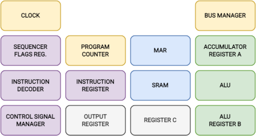
According to the BUS module design and thanks to the modular architecture, you can reorganize the myCPU modules plugging them among different physical layouts. This feature lets you customize the layout of your myCPU more near your preferences. In my case I prefer place the clock module at the bottom of the layout, the BUS manager at the top and the memory block composed by MAR and SRAM modules at bottom as well to get more easy access to switches.
In addition to customize the distribution of the modules, you can choose the orientation of the layout: vertical or horizontal.
At the beginning of the Open Architecture section you could see two images of real layouts.
And below you will find some examples of layouts according to the block modules and module side restrictions:

The horizontal layout needs two flat wires to connect the control bus and data bus between the first two adjacent BUS modules and assembly male connectors instead the female connectors on the sides connected by the wires.
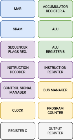
The modules
The myCPU architecture design include 16 functional modules, in this first release, provided through 15 physical module boards in the Kit because the sequencer and the flags register were designed on the same physical module board.
Below you can see the list of physical modules:
- BUS/Power Supply (the main module)
- BUS Manager
- Clock
- Control Signals Manager (CSM)
- Program Counter
- ALU Accumulator Register A
- ALU Operand Register B
- ALU
- Register C
- Output Register
- Memory Address Register (MAR)
- SRAM
- Sequencer + Flags Register
- Instruction Register
- Instruction Decoder
Navigate to Introduction page of modules for more information related to the myCPU modules and the module design in the open architecture.
Display Modules
The myCPU design include, in the first release, two display modules: one for display 8-bit binary values over common leds, and the other one to display a decimal number value over 7 segments digits.
- Decimal number display 4 Digits
- 8-bit Led binary display
You can see a better description of each module on its specific pages: Decimal number display 4 Digits and 8-bit LED binary display
Extra Modules
The myCPU design include two additional modules: An EEProm programmer module for the AT28C64 EEProm memory and a Protoboard module for your custom module prototypes. The protoboard will be provided in the two side versions in the myCPU Kit.
You can see a better description of each module on its specific pages: EEProm programmer module and Protoboard
Features and Limitations of the myCPU
Below you can find the digital features and limitations of my CPU, some features are improvements over the Ben’s eater breadboard computer and other features are obvious derived of the basic nature of the myCPU, but I think could be interesting recognize them too:
Features
Digital features of my CPU
- 16-bit data BUS
- 32-lines control BUS, including power supply connections, status flags, clock and reset signals
- Microinstruction length up to 22 direct control signals
- Instruction cycle from 5 up to 8 cycles
- CISC instruction set type approach
- Von Neumann BUS architecture approach
- Two state flags
- Single clock cycle debugging support, including HIGH and LOW edges
- BUS test switches
- Control Signal test switches
- Microprogrammed instruction decodes
- Clock speed from 5-10 Hz to 3 kHz
- +- 127 programmable integer display mode by a control signal
The Buses
The myCPU uses two buses to share data and connectivity between modules and logical blocks: a Control BUS and a Data BUS. It uses a Von Neumann BUS architecture approach because data and memory addresses share the same BUS: the Data BUS. Really, some of these features are due to the very basic nature of the myCPU design but it very interesting, to students and learners pay attention to this point. Exist another approach, the Harvard architecture which use a dedicated BUS for data and memory addresses.
The myCPU has a shared Data BUS, up to 16 bits, for data and addresses, but only 8-bit are used, in this first release, because all logic devices included, in the myCPU design, support just up to 8-bits.
All the myCPU control signals goes through the Control BUS. The Control BUS has support to 32 lines length over a 32-pin connector, but not all of them are used by control signals. The voltage regulators placed in each BUS module uses pins GND, and +5v of the control BUS to supply power to modules. Clock, Reset signals, also, goes through the control BUS and the Status Flags signals as well.
The lines included on the control BUS are distributed as indicated below:
- Up to 22 control signals
- 2 clock signals: CLK, /CLK
- 4 flag signals: FV, FZ, FN, FC, only the first two of them are used in this release
- 1 HLT signal: HLT
- 2 reset signals RST, /RST
- Power Supply lines: +5v and GND
The 22 control signals are handled by the CSM module (control signal manager) which set the right digital state for each one when connected to each logical element of the myCPU.
The Control Signals of myCPU
The myCPU support up to 22 control signals which control the logic devices of myCPU. Control signals are described deeper at the CSM module page.
The next list shows the function of each control signal and the corresponding logic device:
- CLK, /CLK: clock signals
- RST, /RST: reset signals, myCPU need both signals High and Low.
- HLT: Pause signal, used by the clock module to block the clock signal.
- UN: Signed/Unsigned control of the view mode of 4 digits decimal display.
- AI, AO: Accumulator register load and output.
- BI, BO: Operand register load and output.
- CI, CO: General purpose register C load and output.
- II, IO: Instruction register load and output.
- FI: Flags register load.
- MI: MAR (Memory address register) register load.
- RI, RO: SRAM load and output.
- PE: Program counter increment signal.
- PI, PO: Program counter load and output.
- SI, SO: Stack pointer control signals or to other purposes.
- OI: Output register load.
- EO: ALU Output.
- SU: ALU Subtract mode enable.
- FC, FV, FN, FZ: Flags. Carry, Overflow, Negative and Zero flags.
The Instruction Cycle
The myCPU instruction execution is based on unique Instruction cycle, composed by a Fetch cycle and an Execution cycle. The instruction cycle could have a length from 5 up to 8 states. Each state or step involve one clock cycle and executes only one microinstruction.
Next image shows an example of the instruction cycle for the ADD instruction:

The myCPU support a microinstruction length up to 24 bits, involving 22 control signals.
More advanced and modern CPUs, support more than one instruction cycle per instruction and variable instruction cycle length with dozens of states or steps. The myCPU is based, in its first release, on a fixed length instruction cycle, so an instruction could have an execution cycle with empty states, and it means wasted timings. I’ve planned to implement a variable length instruction cycle, in the next release of the project, by providing an improved set of modules for the instruction processor block.
Because the instruction decoder uses the current state number to decode the corresponding microinstruction for an instruction, the increment of the possible number of states affects to the complexity of the instruction decode process. So, incrementing the number of the states and implementing a variable instruction cycle length is not an simple upgrade but I think it’s mandatory to approach to a more real CPU and is planned for the next version.
Due to the microinstruction based nature of the myCPU, the instruction architecture of myCPU could be described as CISC (Complex Instruction Set Computer) instead of a RISC (Reduced Instruction Set Computer). Each instruction could consumes from 1 to 8 execution state cycles, and probably, it will be upgraded up to 16 state cycles in next release.
The Flags
The myCPU design include up to 4 status flags, but only two of them are used. Mainly for the limitations on the ALU, which is based on simple adders. The first release includes only: a flag for “Overflow”, which correspond with the last carry bit of the adders, and a flag for “Zero” which is calculated by a set of logic gates.
The corresponding control signals are listed below:
- FZ: Zero flag
- FV: Overflow flag
Signed Integer display support
The myCPU support a signed mode of execution, its affects basically only to the mode on how the decimal number display shows numbers. Not affects to the execution itself. There’s a control signal “UN” which tell displays in which mode must display numbers.
This mode has not effect on how ALU perform calculations, only the mode on how numbers are displayed.
When UN control signal is low, decimal displays show numbers unsigned from 0 to 255, and when UN control signal is high, decimal displays show numbers in two’s complement form in a range from -128 to +127 including sign symbol. This behavior was added in this way to keep the same functionality from the Ben Eater’s project and take advantage of his awesome video lectures explaining the two’s complement arithmetic and the build of a decimal 4 digits 7 segment display.
You should watch: Two’s complement arithmetic
Testing using the built-in test switches
The myCPU design provide BUS test switches located at the BUS Manager module, to setup the BUS current values. And the Control Signals test switches located at the CSM module, to setup the microinstruction control signals. Using the CSM switches, you can build a real microinstruction and debug the behavior of your myCPU.
These test switches will be essentials during the building process of your myCPU, testing modules and logic elements individually, without the need to have assembled the rest of the modules, or to test an entire functional block. Almost all modules or functional blocks could be tested using the test switches except, probably, the instruction decoder and the sequencer which are independents of BUS content and control signals.
Debugging over each single clock cycle including high and low states
The myCPU Clock module provide a mechanism to run the myCPU at one clock cycle at a time using a push button. Letting you to debug what is happen during each clock cycle.
The Clock module is based in the 555 timer and is the original design of Ben Eater from his 8-bit breadboard computer, which is an awesome approach to a square wave generator with support to see a clock cycle at a time. In addition, the clock module lets you see what happens during the high and low states of the clock signal. This is very interesting because the myCPU is a synchronized system, where the microinstructions are executed during the low state of the clock signal and the changes of the myCPU status occur during the next high state or the next high edge of the signal.
You can see more detailed description about the clock module on its page: Clock Module
Limitations
The limitations of the myCPU design are due two reasons: the first one is to keep a direct reference to the Ben Eater’s breadboard computer project and take advantage of his fantastic video lectures, and the second one is to provide a smooth learning path to beginners, unexperienced electronics hobbyists or students.
The myCPU design try to maintain a direct correspondence with the Ben Eater’s breadboard compute project and take advantage of his great video lectures. Ben Eater’s site
The myCPU is a very limited CPU. As a learning and experimental platform, performance and advanced functionality was not a main objective, so it has very strong limitations which could be improved in the next release myCPU+. The fact to build the myCPU using discrete logic and basic TTL integrated circuits cause several drawbacks in the design, and electrical issues due to the TTL implementation.
The ALU was designed using just 4-bit adders with the consequent limitation to adding operations and subtracting using the 2´s complement approach.
The SRAM module is based on the 74SL219 which is a very limited SRAM chip of 16 x 4 bits. The limited available memory, to 16 bytes, restrict other features like the length of the instruction set or the posibility to write more complex or large programs because of the limit to 16 instructions. I understand that the SRAM limit is a hard inconvenient but remember that myCPU is a learning platform and you can learn the basics using just 12 to 14 instructions.
Due to the limitation of SRAM, the memory address register (MAR) has a limit to 4-bit address. Does not make sense make it bigger.
There’s no input ports built-in module and no dedicated control signals for inputs in this release. Although you can design your own 8-bit input register and dedicate, the control signals from other module like the Register C, to the input register. Later you can add to your instruction set a specific instruction to load from the input register into ALU registers. An input register is planned to be included with the next release myCPU+.
Challenge to all builders of myCPU, design you own 8-bit input register using a DIP switch for input data, handle the logic device with the control signals CI,CO, add a new instruction LFI (Load From Input into Accumulator) to your instruction set and finally, program your instruction decoder accordingly.
Some of the limitations, in this release, are listed below:
- Basic ALU supporting only add and subtract operations
- SRAM 16 bytes
- Memory Address length 4-bit
- 4-bit instruction Opcode, supporting up to 16 instructions
- Fixed instruction cycle length
- No negative flag
- No RST control signal
- No input ports
- Only one output port with 8-bit support
- Manual introduction of programs using switches
You must keep in mind that the myCPU is not just a device executing a machine code program, is more like that, myCPU is a platform that let you to show what happens on a digital system, like a CPU, during the execution of a program.
Electronic features of myCPU
The myCPU, because of its PCB based design, include several electronic improvements respect the original breadboard project.
You can review some of these improvements below:
- Power Supply of modules through individual voltage regulators
- Separated displays from the main module through an output connector
- Limited resistors for LEDs
- Pull-down resistors on TTL IC inputs when needed
- Pull-up resistors when needed, or on unused TTL inputs
- Decoupling capacitors on TTL ICs
- 4-Layer PCBs
- Independent PWR, GND layers and separated from signal layers
- A filter capacitor in each module
The Instruction Processor
The myCPU design in based on a microprogramming instruction decode, it means that the decoding process to convert an instruction into its equivalent set of microinstructions is done by the code programmed in a EEProm memory instead using combinational logic.
The instruction processor is a logic block responsible of process and execute an instruction and involves several logic elements:
- Instruction Register
- Sequencer
- Flags Register
- Instruction Decoder
- CSM (Control Signals Manager)
Microinstruction decoding
In the myCPU design, a CPU native instruction (machine code) is decoded to a set of microinstructions which are a single sequence of bits representing a set of control signals which can change the status of the myCPU logic elements in a synchronized way.
Each instruction is composed by two or more microinstructions, and each microinstruction is executed during an individual sequencer clock cycle or step, which is another clock signal but dependent of the main clock signal. In the myCPU design the sequencer clock signal is inverted regard to the main clock signal to avoid issues with the response time of the TTL ICs.
The Sequencer determine the microinstruction execution and the main Clock signal determine de myCPU logic status change.

The Instruction Register holds the current Opcode of the instruction, and the address or value of an optional argument if it was defined in the program.
Another piece in the instruction decode process is the Flags Register, which provide the cpu state flags activated on the myCPU to the decoding process. The myCPU has only two flags in this release: Overflow (FV) and Zero (FZ)
So, the decoded microinstruction to execute will be determined by:
- Opcode (4 bits)
- Sequencer step (3 bits)
- Flags (2 bits)
- Memory Selection (2 bits)
The memory selection bits are used to set from which memory unit will be write (during programming) or read (during decoding) each microinstruction byte. In the myCPU design each microinstruction is composed by 3 bytes handled by 3 memory units. Review the Instruction decoder schematic and the programmer code to understand the memory selection when programming the memory.
These binary values compose an address of 11 bits, the address determine the location of the memory where is the microinstruction to execute correponding to a sequencer state. The decoded microinstuction word is passed to the CSM (control signals manager) which send the right control signals to the logic devices of the CPU.
myCPU Roadmap

Next Modules
The next release of myCPU project, which could be the myCPU+ involved a new set of modules to provide 16 bits data support, 16 bits addressing capabilities which give a more bigger SRAM support , up to 64 Kb, support of an instruction set with a length up to 64 instructions, support of CISC instruction type mode with a sequencer length up to 16 steps, support of variable instruction cycle length, more state flags, SRAM program loader, more output ports, input ports support, and many more…
You will find below, a list of planned modules:
- MAR 16 bits
- Register 8 and 16 bits
- Program Counter 16 bits
- SRAM 64K x 8 bits
- Stack Pointer 8 bits
- Instruction Cycle up to 16 states and variable length
- Improved ALU based on 74LS181
- Up to 8 bits flags register
- Instruction Register 8 bits
- CSM with more control signals support
- Input Register 16 bits with two ports
- Output Register 16 bits with two ports